
Your Photonics Product Development Partner
Creating integrated photonic products is hard. Through the U.S. Economic Development Administration’s Regional Technology and Innovation Hubs program (Headwater Tech Hub), we provide startups and established companies a clear, cost-effective path to production.
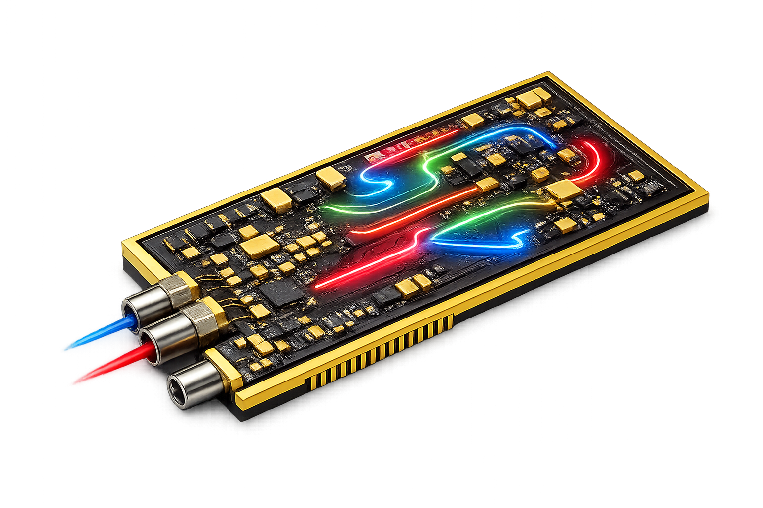
Lab to Market Focus
Specializing in early photonic integrated circuit products
Fast Delivery
From product demonstration to volume manufacturing-ready
U.S. Supply Chain Resilience
Domestic infrastructure
Expedited Integrated Photonics Product Development
Creating cost-effective and scalable products using integrated photonics is challenging.
Except for simple designs a PIC translation is hard—resulting in a process that is long and expensive.
We expedite this process by providing the expertise needed to rapidly translate between "legacy" photonics and integrated photonics.
Core Services
Product Development
Our deep expertise in photonics, systems, and program management accelerates commercialization. We help companies identify needs, recommend changes to speed ramp-up, and connect with expert design, fabrication, packaging, and testing resources for faster ROI and a seamless onramp to the U.S. market.
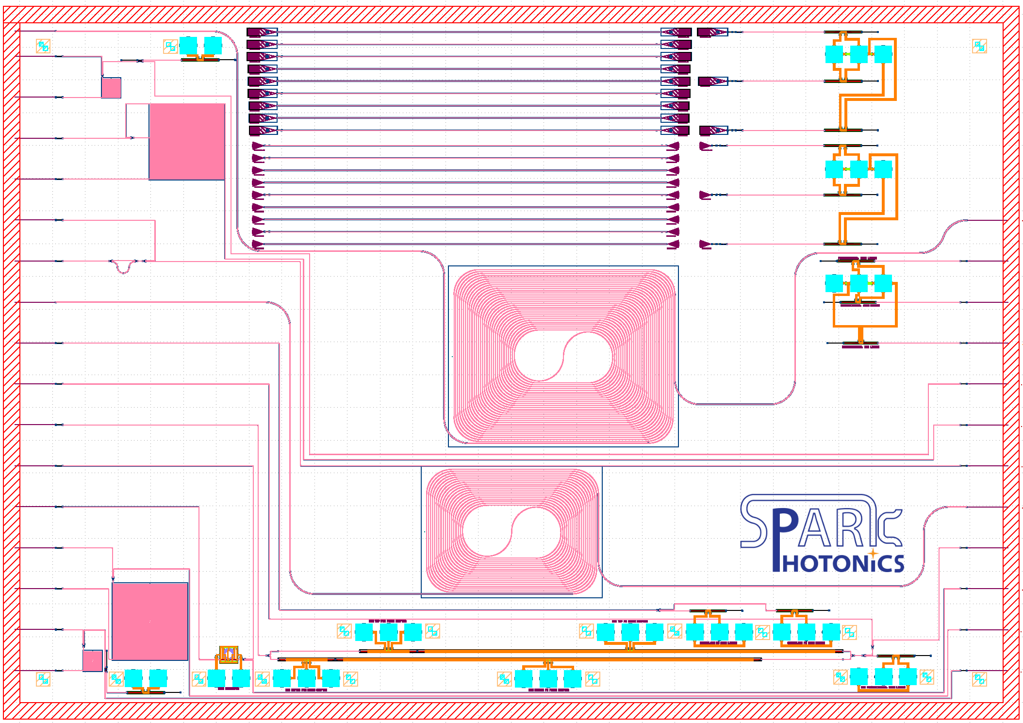
Design
Our experts engage early in the design process to help define specifications, establish architectures, and design for test and manufacture.
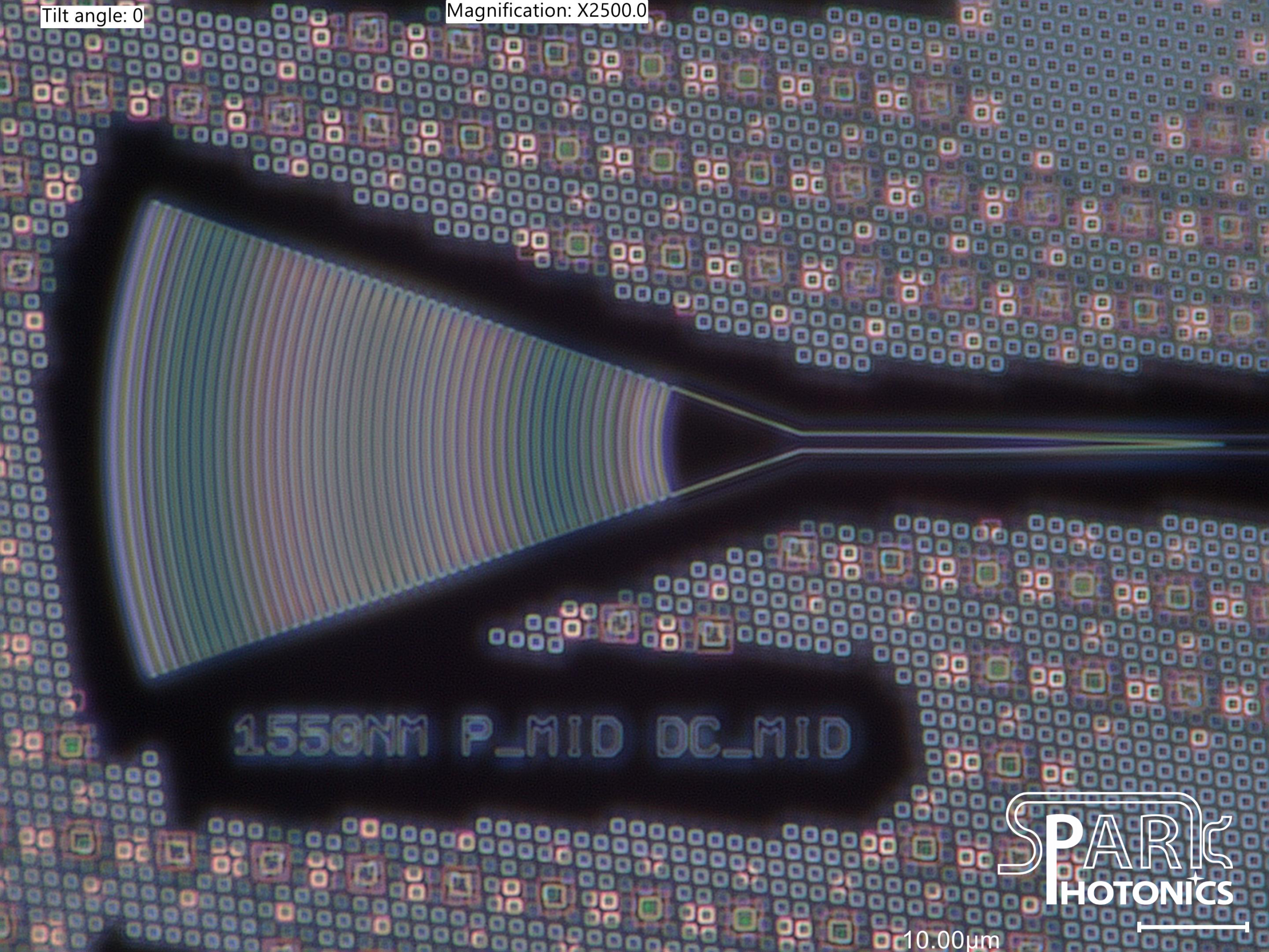
Fabrication
Our relationships with leading foundries across the globe help identify the right solution.
Packaging
We maintain partnerships with US-based photonic packaging services.
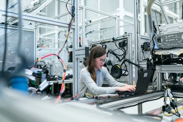
Testing
Our partner services provide component, functional, and environmental testing, as well as system integration and field validation.
Infrastructure
Built for Photonics
Our network of partners house state-of-the-art equipment for integrated photonic product development and test, ranging from wafer-level test all the way to application testing.
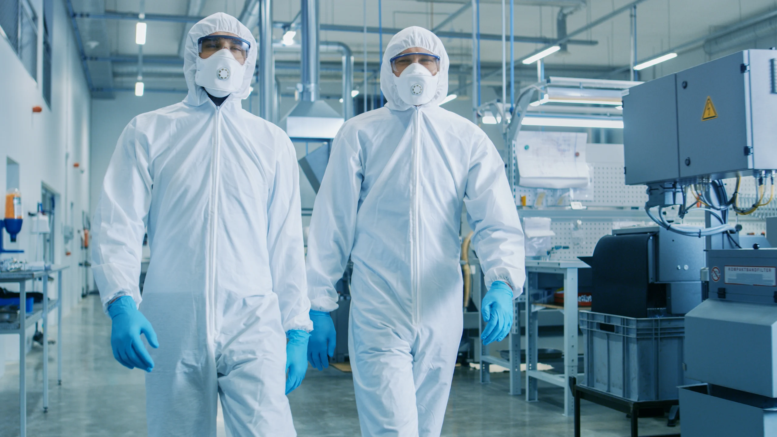
Photonic Packaging
Fiber-chip alignment from single fiber to fiber arrays, die bonding, and enclosure seal.
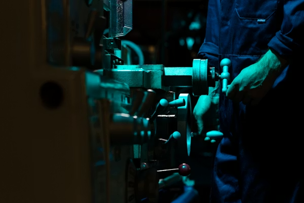
Micro & Nano Fab
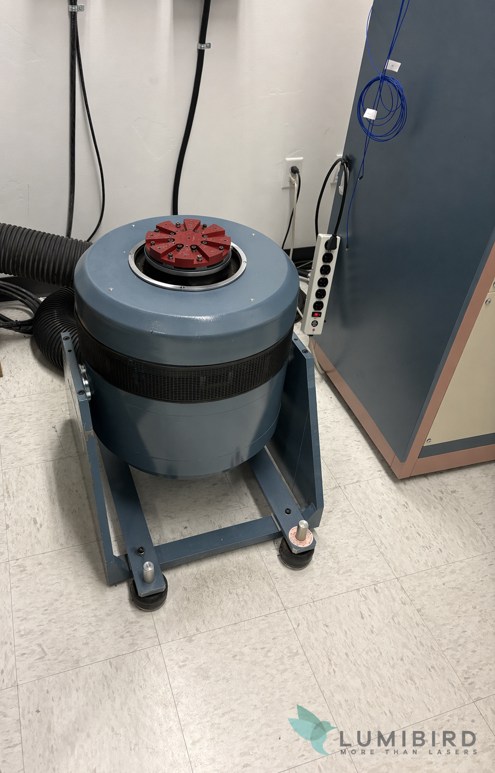
Temp and Shock&Vibe
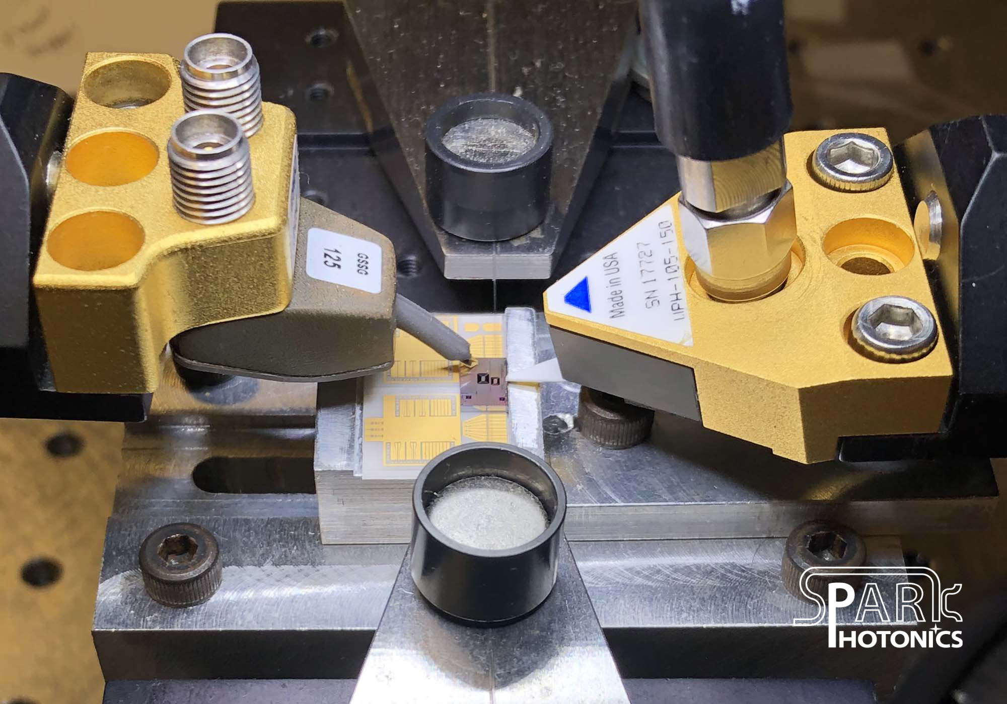
Wafer, Die, and System Test

Precision Ag, GPS-Denied, Forestry
Applications
Industry Sectors
We support customers developing products in high-value, strategic markets.
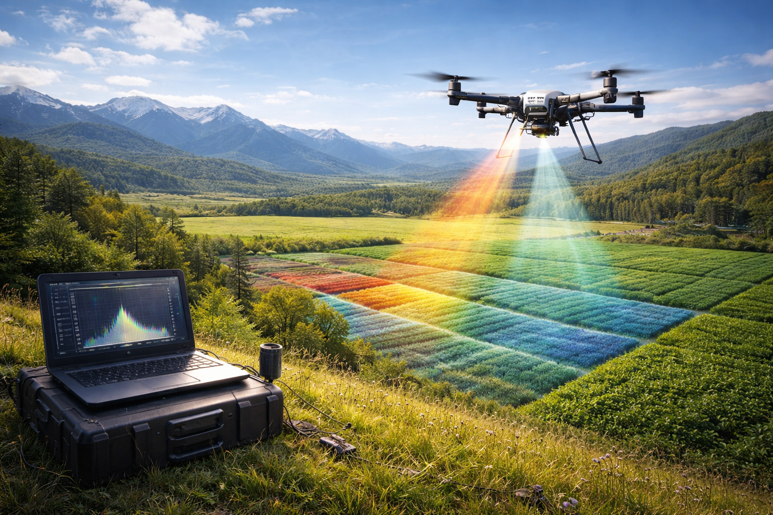
Remote Sensing
Remote Sensing
Photonic sensors redefine how we observe the world, from satellite-based spectrometers to airborne lidar arrays, environmental monitoring systems, and autonomous vehicles.

Defense
Defense
Forward operations with attritable technologies in autonomy, target identification & designation, and secure communications.

Quantum Technologies
Quantum Technologies
Integrated photonic solutions for quantum computing, secure communications, and quantum sensing.
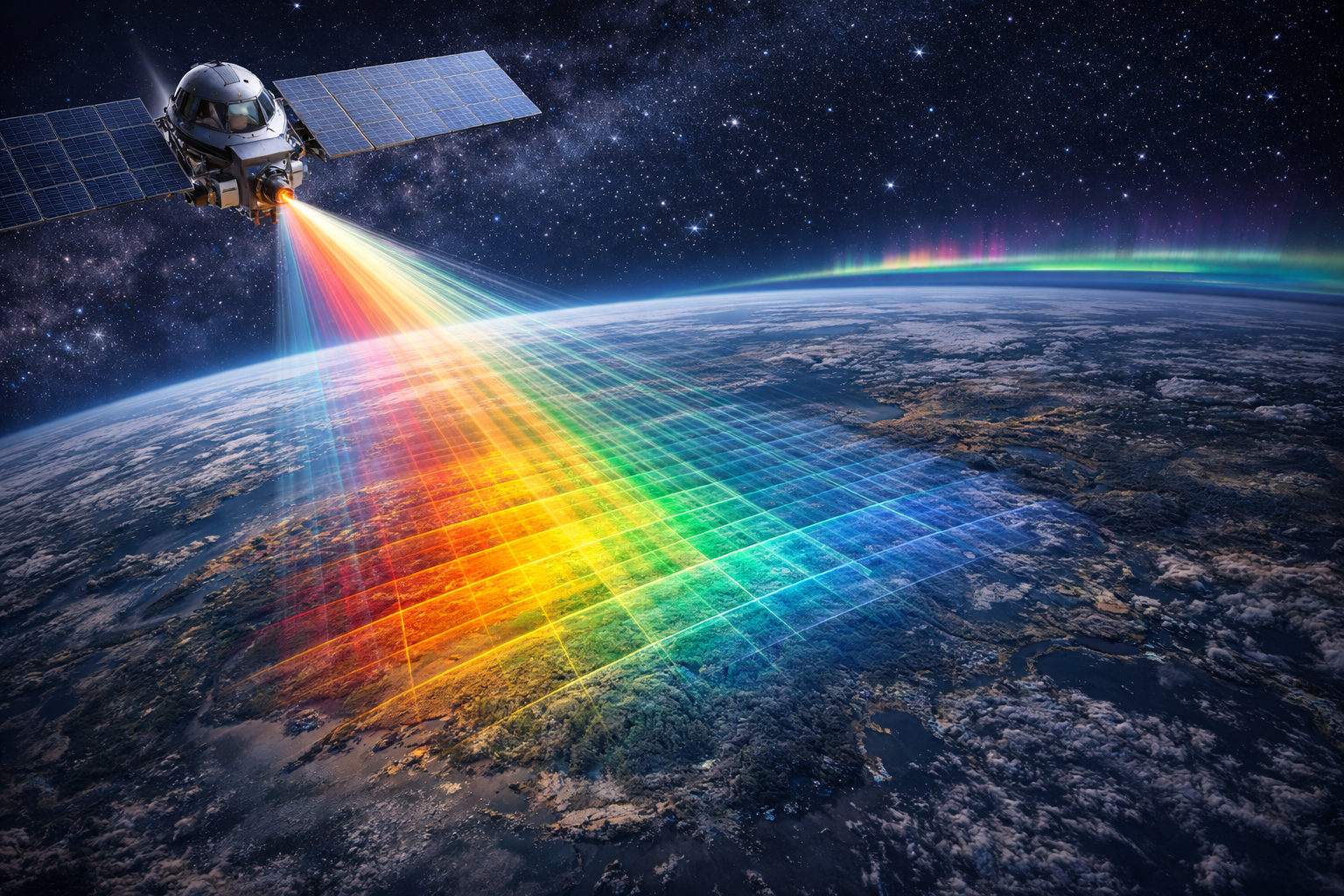
Space Instrumentation
Space Instrumentation
Specialized packaging and rigorous environmental testing for space qualification of optical satellite communications systems and sensors.
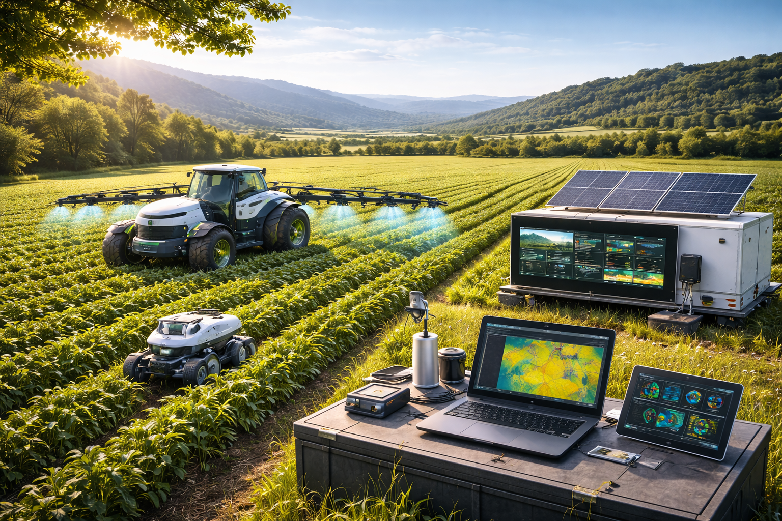
Precision Agriculture
Precision Agriculture
Photonic sensors for autonomy and increased yields with lower costs.
The Ecosystem
Global Network of Trusted Partners
We maintain relationships with commercial, academic, and industrial leaders to ensure a robust, world-class development network and supply chain. Anchored by the Headwaters Tech Hub.